

| Price (4/1/2024) | £1.75 | Estimated Upside | — |
| Market Cap (mm) | £1,270 | EV/EBITDA (trailing) | 17.5 |
| 12-month perf (%) | 75% | P/E (trailing) | 42 |
| 30-Day Avg. Volume | 762,890 | Maint. Capex | 25 |
| 3-Yr Rev Cagr | 106% | Growth Capex | 50 |
| LT Debt (mm) | £189 | Adj. ROIC* | 10% |
| Insider Ownership % | 58% | Adj. FCF Yield* | 3% |
Neutral rating on Alphawave Semi (LSE:AWE) this month. Through extensive research, analyses, and speaking with IR, our initial hypothesis for a “buy” rating did not materialize. Our principle: if we don’t add it to our portfolio, no “buy” rating. Despite lacking excitement, neutral ratings are essential for credibility and track record.
Thesis
We believe two factors are driving the AI megatrend: Higher computation and higher networking needs. AI applications demand high bandwidth and low latency, crucial factors for both training and inference workloads. We believe that AI technology is still in its nascent stages, and are actively seeking companies poised to benefit from this trend. AWE emerged as a compelling prospect, positioned to leverage these evolving networking trends. However, we found evaluating their competitive positioning challenging, especially considering the integration risks associated with their recent acquisitions.
On Connectivity Solutions
AWE specializes in connectivity solutions predominantly in data centers. AWE’s core connectivity offering is Serializer and Deserializer (SerDes), a field in which management has extensive expertise built throughout their 20-year careers. The company’s founders have collaborated for nearly two decades, specializing in connectivity IP at prominent organizations such as Intel.
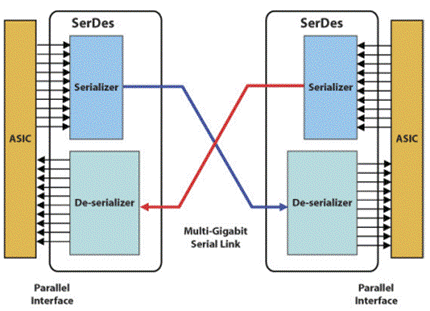
Data centers utilize various methods for connectivity, among which SerDes is a principal technology. SerDes is pivotal for high-speed data transmission. It takes in multiple parallel data streams, combines them into a serial sequence(serialize), transfers the data, upon reaching its endpoint where it gets deserialized in a high-fidelity manner. All of this is to say that SerDes allows for the orderly transfer of large streams of data. Below1 is an illustration demonstrating how one integrated circuit communicates with another using SerDes. SerDes technology is deployed across chips, cabling, and switches, with its specific application varying based on its location within the network architecture. At the switch level, bandwidth emerges as the primary concern for customers. Conversely, when integrated at the chip level, the focus shifts towards minimizing latency, reducing error rate, and optimizing power consumption. While SerDes has been a longstanding component of network infrastructure, the technology underpinning it continues to evolve, catering to high-end applications such as NVIDIA’s NVLink, which facilitates the interconnection of GPUs. SerDes data transmission rates have experienced a significant increase, from 10 Gbps in 2010 to 224 Gbps today, marking a 22-fold growth over fourteen years.
Background
Companies that want to manufacture semiconductor devices require three critical components: silicon intellectual property (IP), software design tools, and a foundry for the production of these chips. Historically, AWE has specialized in providing SerDes IP blocks. These IP blocks can be envisioned as essential building blocks. Connectivity IP is pivotal, often commanding a significant portion of a chip’s size, perimeter, and power consumption due to its role in linking other chips or servers, and accounts for more than 20% of total IP expenditure. Other notable IP categories include those used in CPU and GPU designs. AWE’s IP designs are optimized for speed and low power consumption in data transmission. AWE’s excellence in this field has been recognized repeatedly, with the company receiving multiple awards from foundries like TSMC, which has named AWE the ‘Open Innovation Platform Partner of the Year for High-Speed SerDes’ for four consecutive years.
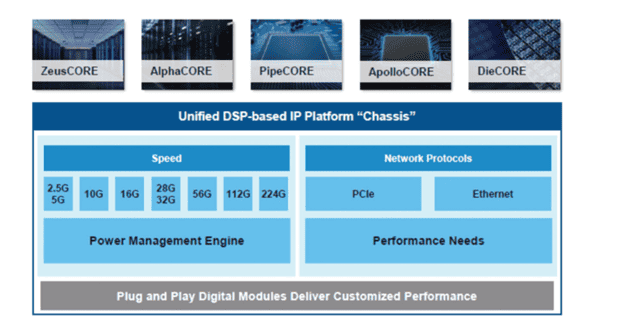
AWE’s SerDes architecture utilizes digital signal processing (DSP), capitalizing on technology scaling to achieve higher bandwidth and accelerated data transmission rates. This versatility allows it to be implemented in various networking standards, including Ethernet and PCIE. The ubiquity of their SerDes technology is noteworthy; it is integral to electrical cables, optical cables, and the interfaces between optical modules and chips. Additionally, it facilitates communication between chips on a board and between dies within a chiplet. The illustration below demonstrates the “chassis” that enables AWE to tailor their SerDes to fulfill a wide array of requirements.
AWE is the fourth largest IP provider in the world (ahead of them are Cadence, Synopsys and Arm). Alphawave’s business model does not involve direct sales to the end customer but rather, it caters to semiconductor companies or foundries that manufacture the chip. The end customers employ design software from companies like Cadence and Synopsys to build their chip. This software enables them to select the appropriate IP blocks and then send their design to a foundry, like Samsung or TSMC, to fabricate the chips. Although AWE’s IP is leading in certain categories, not owning the customer relationship directly makes it difficult to break into the market. Juggernaut design software providers such as Synopsys bundle their IP with their software and strategically leverage their customer relationships to make it more cost-effective and convenient to go with their offerings instead of discrete IP players such as Alphawave. In response to this dynamic, AWE has acquired several companies in recent years to enhance direct engagement with customers and further leverage its IP portfolio.
Strategic Positioning
In 2022, AWE expanded its portfolio through the acquisition of OpenFive, a third-party custom silicon design firm. The company has a team of 300 specialists and has completed over 350 designs and shipped more than 150 million Application Specific Integrated Circuits (ASIC), maintaining an impressive defective parts per million (DPPM) rate below 25. The average selling price of these ASICs ranges from $20 to several hundred dollars.
By bringing design in-house, AWE can bundle its IP, offering customers pre-integrated and verified solutions that provide greater value than standalone IP components. Approximately 30% of the expenses associated with chip design are attributed to the validation, qualification, and verification of IP with the remaining 70% of costs dedicated to tooling and design. The 30% are direct costs that AWE can reduce for customers through prequalified IP blocks. AWE’s go-to-market strategy will likely target smaller companies or larger companies looking for a second source option to the incumbents. Broadcom is currently the stalwart in the custom silicon space with Marvell in second place with revenues of $10B and $2B respectively. NVDA has also entered the foray recently as well.
Alphawave has repositioned OpenFive to focus on leading edge semiconductors, with nearly 90% of its project pipeline dedicated to designs at 5-nanometer technology nodes and smaller. However, why is now an opportune time for the chiplet (more below) industry? Why haven’t other IP providers gone into this space? The IP business boasts one of the highest gross margin business on the planet and could Alphawave simply be impairing their profitability in order to grow.
Chiplets
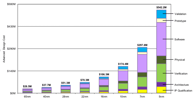
A chiplet is a set of specialized chips designed to work collectively, enabling a more flexible and powerful final product. The chiplet industry is currently in the early stages, particularly as the limitations of Moore’s Law become increasingly apparent. With semiconductor technology now advancing to 3nm geometries, the expense associated with designing chips has escalated significantly. The design costs for a single 5nm integrated circuit can reach upwards of USD $550 million, marking an almost 2x increase from the previous 7nm generation2. This rise in costs encompasses all aspects of chip development, from validation to prototyping. Additionally, manufacturing these advanced chips is becoming prohibitively expensive, as the defect rate for monolithic chips—or single-chip solutions—increases markedly with the move to leading-edge technologies.
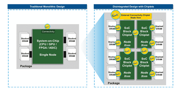
The emerging solution to these mounting costs and challenges is the adoption of chiplets. As the advancement of traditional monolithic chip designs slows, the demand for specialized chips that can efficiently interconnect is on the rise. In response to this need, the Universal Chiplet Interconnect Express (UCIE) standard has been developed, aiming to standardize the communication protocols between chiplets, specifically focusing on die-to-die interconnects. These interconnects act as ‘highways’ that facilitate data transfer between chips, making communication a critical aspect of chip design. Customers can focus on building out their core differentiator whether that be a GPU or DPU, and can outsource the remainder of the chip design. This increases the need for communication as now all the parts in the chiplet need to talk to one another whereas before they were all on the same die. This is where AWE’s IP becomes invaluable; every chip within a chiplet requires a SerDes to establish connections to other chips in the package, making SerDes pivotal in the realm of advanced packaging technologies. One can see how leveraged AWE’s technology is to chiplets in the below diagram. The left hand side represents single monolithic dies and the right hand side displays the many chips in a chiplet.
Opportunities
Data center network refresh
When datacenters go through a switch upgrade, such as the upcoming 51Tb switch, this is tied to overhauls of other networking equipment. As these upgrades are implemented, there will be a heightened demand for cutting-edge SerDes technology, which is essential for supporting the increased data transmission capabilities required by advanced networking infrastructure.
Coherent connectivity
The next step in SerDes is coherent optical solutions. Coherent optics is already used to connect data centers, however, its use within data centers has not been as prevalent due to high costs. This emerging architecture, however, promises highly attractive power consumption characteristics. AWE is seeing significant demand in this segment and currently has a contract with Amazon.
Disaggregated memory
Approximately 30-40% of memory in servers remains underutilized due to overprovisioning. The concept of disaggregated memory addresses this inefficiency by enabling the utilization of memory resources across different servers, thereby optimizing costs. However, the adoption of disaggregated memory necessitates significantly enhanced data transmission capabilities. This requirement expands the TAM for AWE’s products, as their advanced connectivity solutions become increasingly vital for supporting the heightened data transmission demands associated with disaggregated memory configurations.
Artificial Intelligence
In addition to catalyzing the adoption of chiplets, the advancement of Artificial Intelligence (AI) is poised to further elevate demands for enhanced connectivity, reduced latencies, and decreased power consumption. These evolving requirements are expected to significantly propel the growth of the connectivity market in the upcoming years, underscoring the critical role of innovative connectivity solutions in enabling the next generation of AI applications.
Risks
Business Integration
Over the past three years, AWE has expanded its operations through the acquisition of three companies, resulting in a tenfold increase in its workforce. Such rapid expansion and integration pose potential risks to the company’s culture, operational execution, and employee retention.
Exposure to Chinese customers
Among the various factors contributing to the decline in AWE’s share price were the related party transactions with certain customers in China. AWE has been progressively reducing these transactions, yet its revenue from China remains substantial, making up about 40% of revenues in 2023. These revenue streams likely will see significant volatility in the interim with large effects on profitability.
Competitive Landscape
AWE faces substantial competition in the intellectual property (IP) domain from Synopsys and in design services from Marvell and Broadcom. To navigate this competitive landscape, AWE must either achieve technological leadership or adopt a distinctive go-to-market strategy compared to these larger entities. This might involve focusing on different market segments and price points, enabling AWE to carve out a niche within the broader market and effectively differentiate itself from its competitors.
Conclusion
While the prevailing trends are highly favorable for Alphawave, evaluating their competitive edge against established incumbents remains challenging given their status as a newer market entrant and the associated execution risks. Currently, we maintain a neutral rating towards Alphawave, however, this can evolve towards a Buy Rating should we observe clear indicators of successful execution and an uptick in customer engagement. Such indicators would notably include securing IP or chiplet design wins with major hyperscale companies. Achievements of this nature are crucial for affirming Alphawave’s technological prowess and solidifying its leadership within the industry. These milestones would underscore Alphawave’s capacity to adeptly meet market demands and effectively compete within its industry’s dynamic landscape, painting a more optimistic outlook for the company’s future.
Sources:
- https://www.design-reuse.com/articles/10541/multi-gigabit-serdes-the-cornerstone-of-high-speed-serial-interconnects.html
- https://semiwiki.com
INVESTMENT DISCLAIMERS & INVESTMENT RISKS
Past performance is not necessarily indicative of future results. All investments carry significant risk, and it’s important to note that we are not in the business of providing investment advice. All investment decisions of an individual remain the specific responsibility of that individual. There is no guarantee that our research, analysis, and forward-looking price targets will result in profits or that they will not result in a full loss or losses. All investors are advised to fully understand all risks associated with any kind of investing they choose to do.